Most solid materials are composed of millions of small crystals, packed together to form a fully dense solid. The orientations, shapes, sizes and relative arrangement of these crystals are important in determining many material properties. Traditionally, it has only been possible to see the crystal structure of a material by looking at a cut surface, giving just 2D information. In recent years x-ray methods have been developed that can be used to look inside a material and obtain a 3D map of the crystal structure. However, these methods have a resolution limit of around 100nm (one nanometer is 100,000 times smaller than the width of a human hair).
Recently, scientists from Risø DTU (Denmark), Tsinghua University (China), Shenyang National Laboratory for Materials Science, IMR (China) and Johns Hopkins University (USA), report a new method for revealing a 3D picture of the structure inside a material. This newly developed technique allows 3D mapping of the crystal structure inside a material down to nanometer resolution, and can be carried out using a transmission electron microscope, an instrument found in many research laboratories.
Samples must be thinner than a few hundred nanometers. However, this limitation is not a problem for investigations of crystal structures inside nanomaterials, where the average crystal size is less than 100 nanometers, and such materials are investigated all over the world in a search for materials with new and better properties than the materials we use today. The ability to collect a 3D picture of the crystal structure in these materials is an important step in being able to understand the origins of their properties.
An example of such a 3D map is given in the figure, showing the arrangement of crystals in a 150nm thick nanometal aluminium film. The crystals have identical lattice structure (arrangement of atoms) but they are orientated in different ways in the 3D sample as illustrated by the labels 1 and 2. The colours represent the orientations of the crystals and each crystal is defined by volumes of the same colour. The individual crystals of various sizes (from a few nm to about 100 nm) and shapes (from elongated to spherical) are clearly seen and mapped with a resolution of 1 nanometer.
An important advantage of such 3D methods is that they allow the changes taking place inside a material to be observed directly. For example, the mapping may be repeated before and after a heat treatment revealing how the structure changes during heating. This new technique has a resolution 100 times better than existing non-destructive 3D techniques and opens up new opportunities for more precise analysis of the structural parameters in nanomaterials.
This work was reported on May 13th 2011 in Science 332(2011)833.
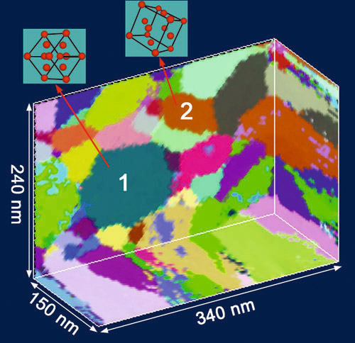
A 3D map of an aluminum composed of nanometer-sized crystals. The crystals have identical lattice structure (arrangement of atoms) but they are orientated in different ways in the 3D sample. Examples of the differently oriented lattices in two crystals (labeled 1 and 2) are illustrated.