Antiferroelectrics, characterized by voltage-driven reversible transitions between antiparallel and parallel polarity, are promising for cutting-edge electronic and electrical power applications. Their electric dipoles are believed to be antiparallel arranged along specific directions, which are similar to the antiferromagnets and thus cancel the possible, spontaneous polarizations on the macroscopic scale.
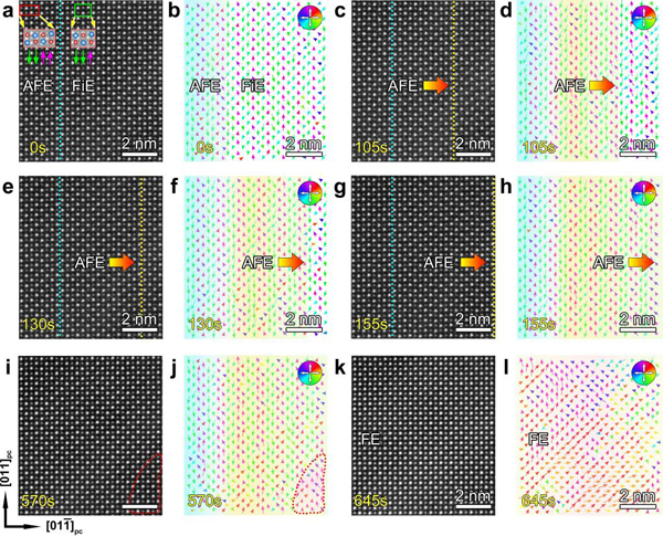
Here, a novel ferrielectric dipole configuration with both angular and amplitude modulations was found in the classic PbZrO3 antiferroelectric films, which was further identified as the role of precursor for subsequent antiferroelectric to ferroelectric phase transition. Basically, this ferrielectric phase displays ↑↑↓ periodic polar structures other than the ↑↑↓↓ antiferroelectric polar modulations in the antiferroelectric matrix. In particular, with the participation of this ferrielectric phase, the phase transition pathways driven by phase boundary have been demonstrated. Based on atomic-resolution transmission electron microscopy, the underlying atomic level details in these PbZrO3 films were elucidated. These results were reported in Nano Letters. with the title of “Atomic insight into the successive antiferroelectric-ferroelectric phase transition in antiferroelectric oxides”.
This work challenges the long-standing recognition of the antiferroelectric-ferroelectric phase transition model in low-dimensional PbZrO3. These results will provide new viewpoint to understand the antiferroelectric materials and related properties on the atomic scale, which will be important for studying and revealing the phase transformations and responses in low-dimensional PbZrO3 films and thus will prompt the development of antiferroelectric-based nano-electronics.

Fig 1. Ferrielectric-antiferroelectric-ferroelectric phase transition process and related first-principle calculations. (a) phase transition process. (b) energies of different phases. (Image by IMR)

Fig 2. Phase boundary-driven phase transition in PbZrO3 films under the irradiation of electron beam. (a, c, e, g, i, k) atomic-scale HAADF-STEM images series. (b, d, f, h, j, l) corresponding Pb2+ displacement mappings. (Image by IMR)
Nano Letters: https://pubs.acs.org/doi/10.1021/acs.nanolett.2c04972?ref=pdf
