Chinese scientists have developed high-performance n-type Mg₃(Sb, Bi)₂-based thermoelectric thin films through a novel dual-defect engineering strategy, addressing key challenges that have long hindered their application in miniaturized energy harvesting devices.
Thermoelectric materials, capable of directly converting heat into electricity, hold great promise for powering Internet of Things (IoT) sensors through waste heat recovery and for solid-state cooling applications. Among various material systems, n-type bulk Mg₃(Sb, Bi)₂-based compounds have attracted attention due to their abundant, environmentally friendly constituents and excellent thermoeletric properties.
However, research on their thin-film counterparts has significantly lagged due to two major obstacles: the difficulty in controlling composition during deposition caused by high magnesium vapor pressure, which creates detrimental magnesium vacancies; and the complexity of achieving effective doping in thin films to optimize carrier concentrations. The aforementioned issues have severely hindered the optimization of the thermoelectric performance of Mg₃(Sb, Bi)₂ thin-film materials, thereby limiting their application in the Internet of Things (IoT).
Researchers led by Prof. TAI Kaiping from the Institute of Metal Research, Chinese Academy of Sciences (IMR, CAS), overcame these obstacles using multi-target magnetron co-sputtering. Their dual-defect engineering strategy combines two synergistic approaches: introducing excess magnesium during deposition to suppress the formation of electron-killing magnesium vacancies, and precise tellurium (Te) substitution of bismuth to introduce additional electrons for fine-tuning carrier concentration.
The optimized Mg₃.₁₅Bi₁.₄₆Sb₀.₅Te₀.₀₄ thin film achieved a peak thermoelectric figure of merit (zT) of 0.47 at 525 K, representing a 114% enhancement over p-type Mg₃(Sb, Bi)₂ films. Atomic-scale characterization revealed that Te doping not only optimizes carrier concentration but also induces lattice strain and dislocations that enhance phonon scattering, suppressing thermal conductivity by over 53% compared to p-type films.
Demonstrating practical potential, an all-Mg-based prototype device incorporating the optimized films generated an output voltage of 73 mV and power density of 1185 μW cm⁻² at a 120 K temperature difference, showcasing capability for micro-power generation in mid-temperature range applications.
The research, published in Acta Materialia, establishes a universal design principle for thin-film thermoelectric materials and bridges the critical performance gap between bulk and film systems.
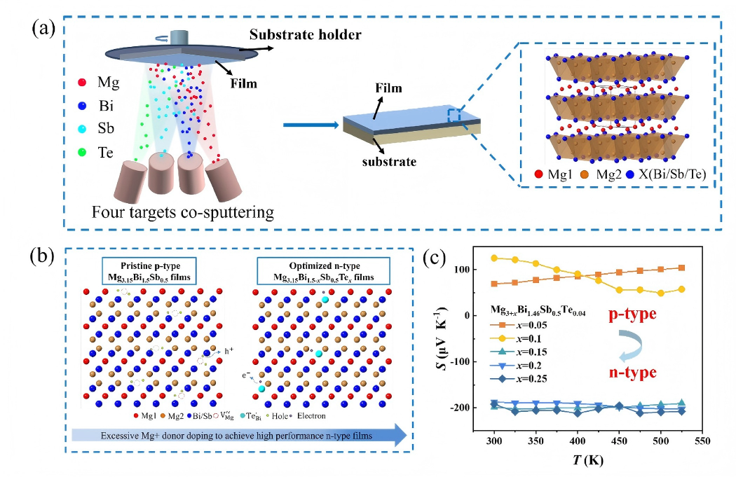
Schematic illustration of the fabrication process for n-type Mg₃(Sb, Bi)₂ thin films and the mechanism of p-type to n-type transition. (Image by IMR)
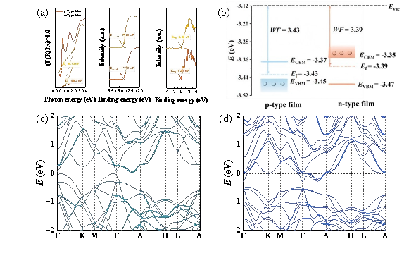
Comparison of band structures between n-type and p-type Mg₃(Sb, Bi)₂ thin films: (Top) Experimental characterization results; (Bottom) DFT calculation results. (Image by IMR)
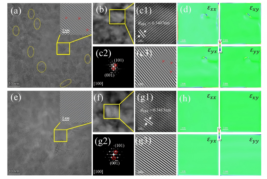
Comparison of microstructural characterization between n-type (a-d) and p-type (e-f) Mg₃(Sb, Bi)₂ thin films. (Image by IMR)
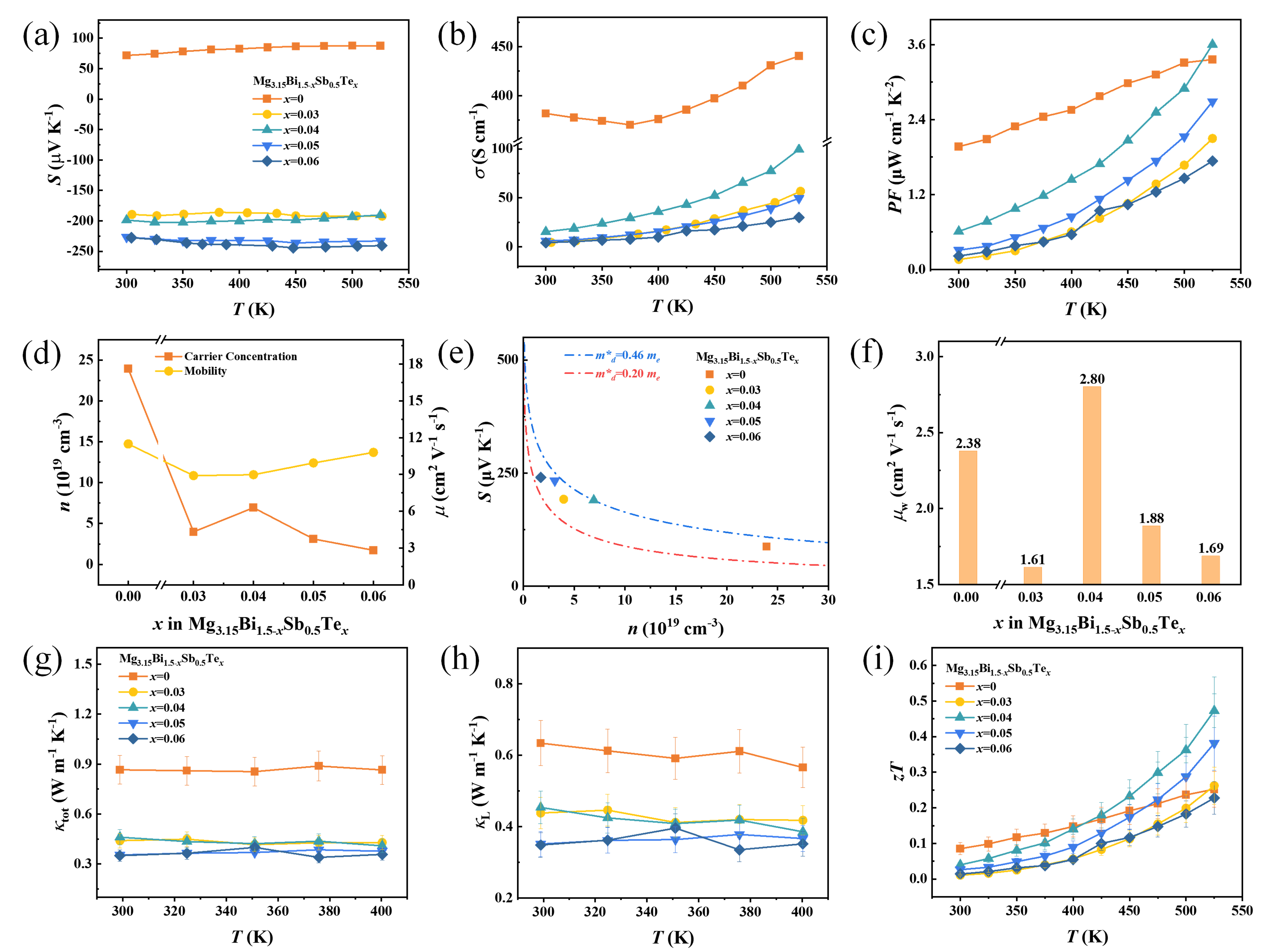
Electrical transport properties of n-type Mg₃(Sb, Bi)₂ thin films. (Image by IMR)
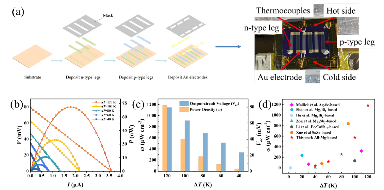
(a) Fabrication process of the all-Mg-based thin-film thermoelectric device, and (b-d) characterization of its power generation performance. (Image by IMR)