Title:“Tracking the ‘Birth’ of Charge Carriers in Nanomaterials by THz Spectroscopy” 太赫兹谱学:纳米材料载流子觅踪
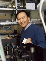
Speaker:Prof. Hai WANG 王海
Institute:Max Planck Institute for Polymer Research 德国马普聚合物研究所
Venue:Room 406, Shichangxu Building 工艺楼406
Time:13:30 PM, 06th April. 4月6日(周四)下午13:30
Abstract: The conversion of light into electrical currents is a fundamental process underlying the operation of varied optoelectronic devices including photovoltaics and photodetectors. Understanding the underlying photophysics, e.g. generation and transport of charge carriers in the photoactive materials following photoexcitations, is crucial for improving the energy conversion efficiency of devices.
Layered two-dimensional (2D) materials are emerging building blocks for the next generation electronics and optoelectronics. Since the discovery of graphene, the family of the 2D materials have been largely expanded, converging the metallic (e.g. graphene), semiconducting (e.g. transition metal dichalcogenide) and insulating phases (e.g. hexagonal boron nitride). The recent emergence of conductive semiconducting organic layers (e.g. metal covalent organic framework) has further extended the 2D material library and provided new functionalities for applications.
In this talk, I will first provide some basics on ultrafast THz spectroscopy and demonstrate its strength in characterization of electrical transport properties1 of charge carriers, low energy excitations2 in solids and charge transfer3-4 dynamics across interfaces in a contact-free manner for low-dimensional materials. I will then discuss some recent work from us related to the ultrafast “birth” of charge carriers following photoexcitation by photoconductivity studies, with a particular focus on the role of many-body interactions (carrier-carrier, carrier-phonon interactions) in dictating the process of hot carrier relaxation5, transport6, and “lattice-dressing” effect7.
References
1. Shuai Fu et.al, Outstanding Charge Mobility by Band Transport in Two-DimensionalSemiconducting Covalent Organic Frameworks, Journal of the American Chemical Society, 2022, 144, 16.
2. Alexander Tries et.al, Experimental Observation of Strong Exciton Effects in Graphene Nanoribbons, Nano Letters 2020, 20, 5, 2993–3002.
3. Shuai Fu et.al, Long-Lived Charge Separation Following Pump-Energy Dependent Ultrafast Charge Transfer in Graphene/WS2Heterostructures, Science Advances 2021, 7, eabd9061.
4. Shuai Fu et.al, Reversible Electrical Control of Interfacial Charge Flow across van der Waals Interfaces, Nano Letters, 2023, in press.
5. Wenhao Zheng et.al, Photoconductivity Multiplication in Semiconducting Few-Layers MoTe2, Nano Letters 2020, 20, 8, 5807–5813.
6. Heng Zhang et.al, Highly Mobile Hot Holes in Cs2AgBiBr6Double Perovskite, Science Advances 2021, eabj9066.
7. Wenhao Zheng et.al, Band Transport by Large Fr hlich Polarons in MXenes, Nature Physics 2022, 18, 544-550.
Bio
 Dr. Hai Wang studied materials science at Zhejiang University and obtained his degree in 2009. Between 2009 and 2011, he finished a joint master program in nanoscience at University of Leuven (2009-2010) in Belgium and Delft University of Technology in the Netherlands (2010-2011), supported by the Erasmus Mundus fellowship. From 2012, Hai Wang started his PhD at Max Planck institute for polymer research (MPI-P) in Mainz with the support of a fellowship from MAINZ (graduate school of excellence, materials science in Mainz). In his PhD, Hai worked with Prof. dr. Mischa Bonn to investigate ultrafast charge transfer processes at quantum dot and oxide interfaces, and graduated with Summa Cum Laude (with highest honors) in 2016. After spending 1 year in the group of Mathias Kl
 ui at University of Mainz as a postdoc, Hai started his independent research group “Nano- optoelectronic materials” in the Molecular Spectroscopy department at MPI-P in 2017. Employing time-resolved, ultrafast spectroscopies (THz spectroscopy, transient absorption etc.), the central theme of Hai’s current research lies in understanding fundamental charge carrier dynamics and low-energy excitations in solid-state low-dimensional materials and interfaces, relevant for energy and optoelectronic applications.