Grain boundaries (GBs) are intrinsic topological defects of large-area polycrystalline graphene films grown by chemical vapor deposition (CVD). Although the influence of individual GBs has been extensively studied theoretically and experimentally, the real influences of grain size on the thermal and electrical transport properties on a large scale are still not clear because of the difficulty of synthesizing graphene with a tunable uniform grain size that is smaller than the phonon and electron mean free paths (~ a few hundreds of nanometers).
Scientists from the Institute of Metal Research, Chinese Academy of Sciences (IMR, CAS) recently developed a segregation-adsorption CVD method to grow well-stitched high-quality monolayer graphene films with a tunable uniform grain size from ~200 nm to ~1 μm, by using a Pt substrate with medium carbon solubility. Such graphene films enable the determination of the scaling laws of thermal and electrical conductivities as a function of grain size. It is found that the thermal conductivity of graphene films dramatically decreases with decreasing grain size by a small thermal boundary conductance of ~3.8×10⁹ Wm-2K-1, while the electrical conductivity slowly decreases with an extraordinarily small GB transport gap of ~0.01 eV and GB resistivity of ~0.3 kΩ·μm. Moreover, the changes in both the thermal and electrical conductivities with grain size change are greater than those of typical semiconducting thermoelectric materials.
These findings provide valuable information for tuning the thermal and electrical properties of graphene for electronic, optoelectronic and thermoelectric applications through grain size engineering.
The study entitled "Tailoring the thermal and electrical transport properties of graphene films by grain size engineering" has been published in the February issue of
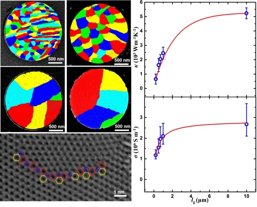
Well-stitched high-quality monolayer graphene films with different grain size and the influence of grain size on the electrical and thermal conductivity.(Image by IMR)