Most conducting materials in bulk exhibit a three dimensional (3D) isotropic electrical conductivity and electrons can flow freely along any of their crystallographic directions. How to construct the highway of electrons in bulk conductors to guide them moving along a designed direction is a subject of fundamental physical interest as well as being important for developing advanced electronic devices. Due to their quasi-one-dimensional (1D) metallic conductivity, the perovskite-related SrnNbnO3n+2 compounds provide us an opportunity to unveil the physical origin for the preferential pathway of electrons.
In a recent study published in ACS Nano, an international research team including Prof. CHEN Chunlin and Prof. MA Xiuliang from Institute of Metal Research, Chinese Academy of Sciences (IMR, CAS), Prof. Johannes Georg Bednorz from Zürich Research Laboratory, and Prof. Yuichi Ikuhara from The University of Tokyo, unambiguously determined the atomic and electronic structures of the SrnNbnO3n+2 compounds and revealed the underlying mechanism for their quasi-1D metallic conductivity.
The perovskite-related SrnNbnO3n+2 compounds are composed of alternately stacked chain-like slabs and zigzag-like slabs. The zigzag-like slabs in all these compounds as well as the chain-like slabs in SrNbO3.5 are electrically insulating because the NbO6 octahedra in these slabs are significantly distorted with a large displacement of Nb from the octahedral centers and the Nb valence is Nb5+. The chain-like slabs in SrNbO3.4 and SrNbO3.45 are conducting since their Nb valence/electron configuration is Nb(5-w)+/4dw with w > 0. The nearly undistorted NbO6 octahedra lead to a metallic conductivity along the a-axis.
Structurally, the SrnNbnO3n+2 quasi-1D conductors can be derived by intercalating the insulating zigzag-like slabs into the 3D conducting SrNbO3 perovskite along {110} planes. Such a concept of segmenting a 3D conductor into a stack of quasi-2D conducting thin layers by inserting insulating layers in between them should be applicable not only to SrNbO3/SrNbO3+y = SrnNbnO3n+2 but also to other materials.
This finding may boost applications of 2D electrical conducting materials and devices.
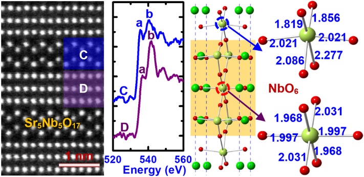
Figure: Atomic and electronic structures of the SrNbO3.4 compound. The NbO6 octahedra in the chain-like slabs are nearly undistorted, while those in the zigzag slabs are significantly distorted with a large displacement of Nb from the octahedral centers. (Image by IMR)