Grain boundary (GB) is one of the most important defects in crystalline materials. In bulk materials, GBs are usually categorized as low-angle and high-angle GBs depending on their misorientation angles. Low-angle GBs (with misorientation angles less than 15°) are usually considered and described by dislocations, while high-angle GBs by structural units. As the diameter of crystals goes below 10 nm, the remarkable interaction between surfaces and GBs may have significant influence on GB structures, but this has not been explored theoretically or experimentally at present.
Recently, Prof. DU Kui’s group in cooperation with Prof. LI Feng and Prof. JIN Haijun from Institute of Metal Research, Chinese Academy of Sciences (IMR, CAS) discovered a significant size effect on the grain boundary structure in sub-10-nm gold nanocrystals through in situ atomic resolution aberration corrected electron microscopy.
It was demonstrated that when the diameter of the nanocrystal is larger than 10 nm, the GB with misorientation angle above 15° exist as dislocation type (DGB) while GB with misorientation angle below 15° exist as structural-unit type (SGB) , in accord with that in bulk metals. However, with the diameter of a nanocrystal decreasing down below 10 nm, the critical misorientation angle between DGB and SGB increases inversely with the diameter of the nanocrystal. Particularly, when the diameter of a nanocrystal decreases to 2 nm, a high-angle GB with misorientation angle up to 28.6° exists as dislocation type. Quantitative strain analysis shows that elastic strain exist around DGBs while not for SGBs; thus the width of a DGB is evidently larger than that of a SGB. In situ deformation experiments indicate that the size-effect-induced DGBs remained stable via migration of dislocation arrays rather than GB sliding, thus it effectively improves the mechanical stability of nanocrystals. Moreover, in situ electrical measurements demonstrated that the electrical resistance induced by a DGB is much less than a SGB, thus it improves the conductive stability of nanocrystals. Therefore, the size effect on grain boundary structure in supernano crystals can simultaneously improve the conductive and mechanical stabilities of nanocrystals. This may be of importance to designing new generation interconnects and nanodevices.
This work entitled "Size-Dependent Grain-Boundary Structure with Improved Conductive and Mechanical Stabilities in Sub-10-nm Gold Crystals" has been published online in Physical Review Letters.
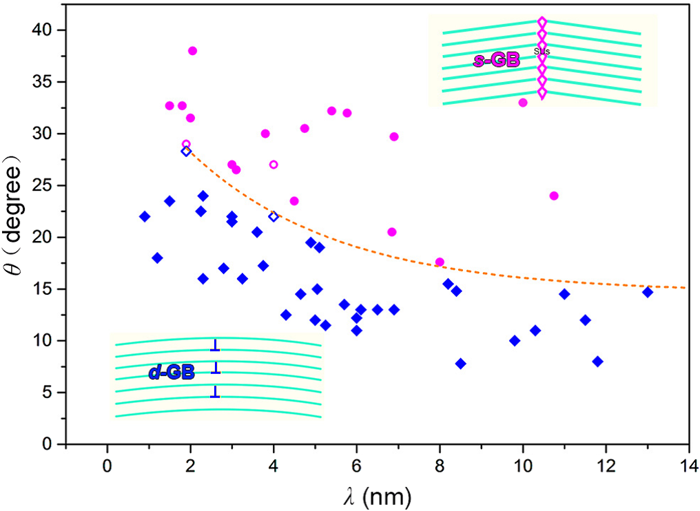
Figure 1. Statistical distribution of two types of grain boundaries with different misorientation angles θ in gold nanorods with diameters λ. (Image by IMR)
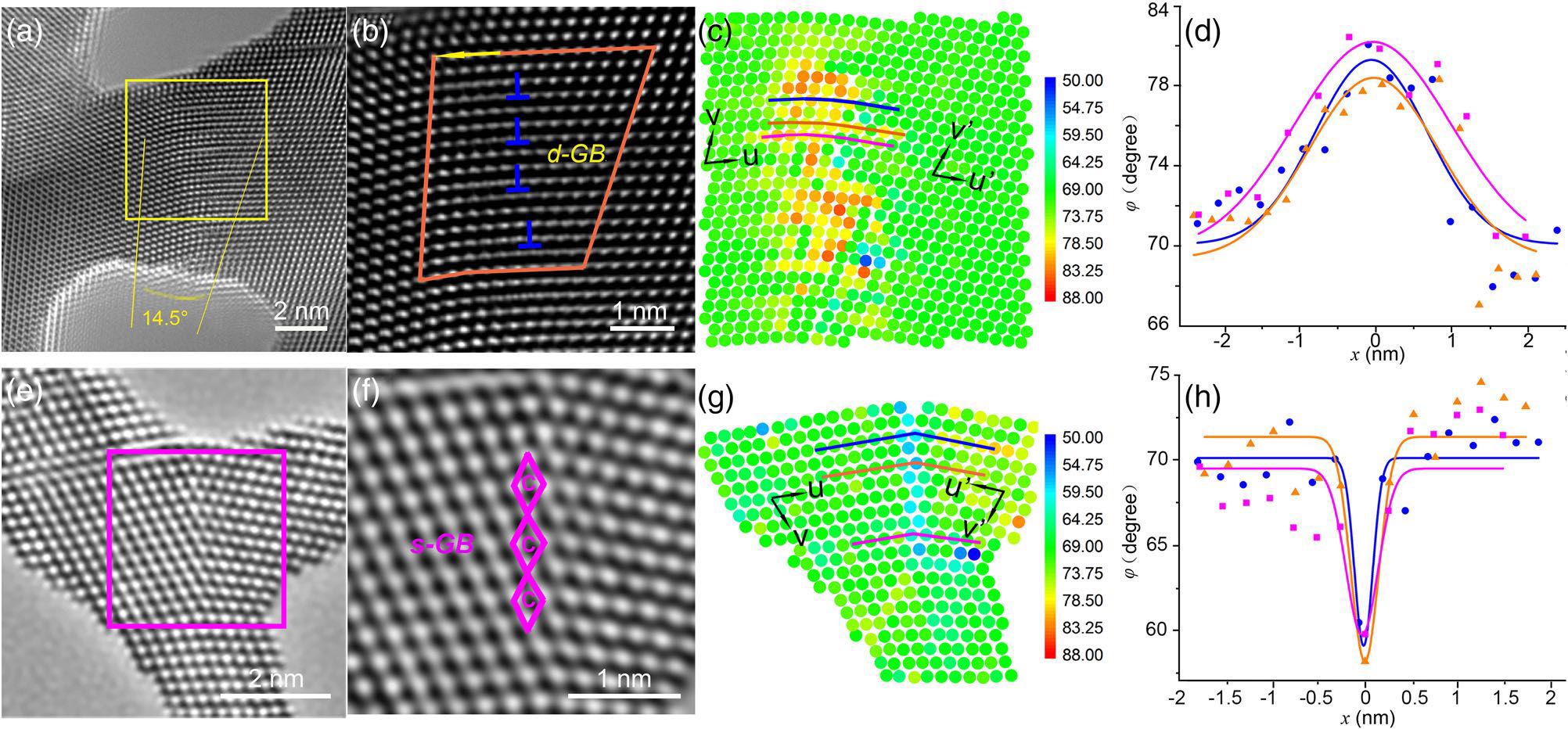
Figure 2. Aberration-corrected high-resolution transmission electron microscopy images and quantitative strain analysis of (a-d) DGB and (e-h) SGB. (Image by IMR)