Transparent conductive films (TCFs) are an important component of touch screens, smart windows, liquid crystal displays, organic light-emitting diodes (OLEDs), and organic photovoltaic cells. Indium tin oxide (ITO) has been the most widely used transparent conductive material, however, the limited reserves of indium and the brittle nature of ITO hinder its sustainable application in flexible electronics. Single-wall carbon nanotube (SWCNT) networks show excellent flexibility, desirable optical properties and good electrical conductivity, and therefore, is a promising candidate for making flexible TCFs. However, the reported optoelectronic performance of SWCNT TCFs are far away from those of ITO TCFs.
It’s well-proven that the intertube junction resistance and bundling effect are key issues limiting the transparent electrical properties of SWCNT TCFs. On one hand, owing to the Schottky barrier at intertube junctions, carrier transport is seriously suppressed, which results in much higher junction resistance than that of individual SWCNTs. On the other hand, SWCNTs with diameters of 1-2 nm usually aggregate into bundles (tens of nm in diameter) by van der Waals interaction to decrease surface energy; as a result, the internal tubes absorb light but contribute little to carrier transport. Therefore, it would be highly desirable to produce SWCNT films with small bundle size and low junction resistance.
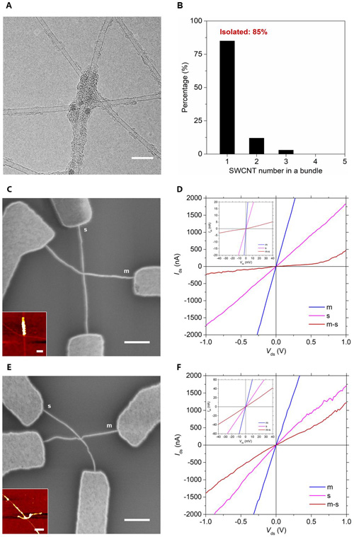
Recently, Prof. CHENG Hui-Ming and Prof. LIU Chang’s group at Institute of Metal Research, Chinese Academy of Sciences and collaborators synthesized a SWCNT thin films composed of isolated SWCNTs with carbon-welded joints for TCF by an injection floating catalyst chemical vapor deposition method (Fig. 1A). By tuning the nucleation and growth concentration of SWCNTs, 85% the SWCNTs are isolated (Fig. 1B); by controlling the content of carbon source, a “carbon welding” structure is formed at tube-tube junctions.
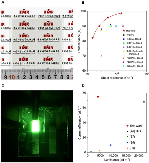
It is demonstrated that the carbon-welded joints convert Schottky contacts between metallic and semiconducting SWCNTs into near-ohmic ones (Fig. 1C-F), which significantly lowers the intertube junction resistance. Due to their unique structure, the pristine SWCNT films show a record low sheet resistance of 41Ω □-1 at 90% transmittance for 550-nm light; after HNO3 treatment, the sheet resistance further decreases to 25Ω □-1, better than that of ITO on a flexible substrate (Fig. 2A-B). The OLEDs constructed using this SWCNT film as anodes demonstrate a high current efficiency of 75 cd A-1, 7.5 times higher than that of the best reported CNT anode–based OLEDs (Fig. 2C-D). The OLEDs also exhibit excellent flexibility and stability.
These high-performance SWCNT TCFs with good flexibility show a great potential for use in various flexible electronic and photoelectronic devices as a transparent electrode.
The main results of this work was published online in Science Advances entitled "Ultrahigh-performance transparent conductive films of carbon-welded isolated single-wall carbon nanotubes".

Fig. 1. Isolated SWCNT network with carbon-welded joints and SWCNT FETs. (A) Typical TEM image. Scale bar, 10 nm. (B) Statistical data of the numbers of isolated and bundled SWCNTs in the network. (C and E) SEM images of two representative SWCNT FETs without (C) and with (E) the carbon-welded joint. Scale bars, 1 μm. The inset AFM images show the deposited carbon (white part) on the SWCNTs. Scale bars, 100 and 200 nm, respectively. (D and F) Ids versus Vds of the device (C) and (E), respectively. Gate voltage Vgs = -10 V. (Image by IMR)

Fig. 2. SWCNT TCFs and OLEDs. (A) Optical image of an 80 mm × 80 mm SWCNT TCF. (B) A comparison of transmittance and sheet resistance of our doped SWCNT TCFs together with the reported results for doped CNT TCFs and the superior ITO TCF. (C) Optical image of a lit SWCNT OLED. (D) A comparison of the current efficiency and luminance of our SWCNTOLED with those of the reported CNT anode–based OLEDs and the best ITO-PET OLED. (Image by IMR)