Meter-scale single-wall carbon nanotube (SWCNT) thin films with an excellent optoelectrical performance has been developed for the first time by Chinese researchers from Institute of Metal Research, Chinese Academy of Sciences.
SWCNTs have been considered one of the most promising candidates for flexible and transparent electronic devices due to their extraordinary mechanical, electrical, and optical properties. The production of high-quality SWCNT thin films by an efficient and scalable method has become a key issue for their practical application in electronics. However, two major obstacles remain for the research and development of macro-electronics based on SWCNT thin films. First, the size of fabricated SWCNT films is usually limited to the square centimeter scale, and the batch processing used is not scalable. Second, the optoelectrical performance of SWCNT films remains unsatisfactory due to the introduction of impurities and structural defects during the fabrication processes. Therefore, the production of high-quality SWCNT thin films by an efficient and scalable process remains a big challenge.
Recently, the researchers from Institute of Metal Research, Chinese Academy of Sciences (IMR, CAS), proposed a continuous synthesis, deposition, and transfer technique for the fabrication of high-quality SWCNT thin films of meter-scale dimension with excellent optoelectrical performance. Large-area, flexible, and transparent all-CNT thin-film transistors (TFTs) and various integrated circuits (ICs) were also fabricated to demonstrate the potential use of these SWCNT thin films in large-area, flexible, and transparent electronics. These results have been published on 28 June, 2018 in Advanced Materials (doi: 10.1002/adma.201802057).
SWCNTs are continuously synthesized by a floating catalyst chemical vapor deposition technique, and then deposited on a moving membrane filter forming SWCNT thin films. The length of the SWCNT film is unlimited, because the as-deposited film is transferred onto a flexible poly(ethylene terephthalate) substrate with the aid of a roll-to-roll transfer system, and the membrane filter can be repeatedly used for the SWCNT film collection. More importantly, as there are no impurities and defects introduced in the production processes, the SWCNT films have an excellent optoelectrical performance including a low sheet resistance of 65 Ω/□ with a transmittance of 90% at a wavelength of 550 nm. Using these SWCNT thin films, all-CNT TFTs and ICs including 101-stage ring oscillators have been constructed that show excellent performance and uniformity.
“The present method enables us first to achieve continuous production including the growth, deposition, transfer and re-deposition of SWCNTs.” the paper’s co-first authors, WANG Bing-Wei and JIANG Song said. “The meter-scale high-quality SWCNT films and the devices fabricated from them will pave the way for future development of large-scale, flexible, and transparent electronics based on SWCNT thin films.”
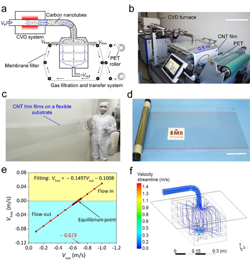
Figure 1. Preparation of meter-scale SWCNT thin films. a) Schematic showing the apparatus designed for the synthesis, deposition, and transfer of SWCNT films. b) A photograph of the home-made apparatus (scale bar, 0.5 m). c) A SWCNT thin film transferred on a flexible PET substrate with a length of more than 2 m. d) A roll of uniform SWCNT thin film on the PET substrate (scale bar, 0.1 m). e) Finite-element simulation of the dependence of Vout on Vfree for an inlet gas velocity Vin = 0.068 m s-1. f) Simulation results showing a uniform velocity distribution in the gas stream in the filtration system at the equilibrium state. (Image by IMR)
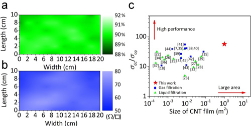
Figure 2. Characterization of the as-prepared SWCNT thin films. a) Transmittance and b) sheet resistance mapping, demonstrating good uniformity of the films. c) A comparison of our SWCNT transparent conductive film with previous results. (Image by IMR)
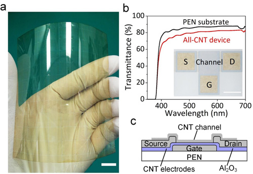
Figure 3. All-CNT TFTs. a) Photograph of all-CNT TFT device fabricated on a flexible PEN substrate. b) Optical transmittance of the PEN substrate (black line) and the all-CNT device fabricated on the substrate (red line). Inset: optical microscopy image of a buried-gate all-CNT TFT (scale bar, 100 μm). c) Schematic cross-section of a buried-gate all-CNT TFT on a PEN substrate. (Image by IMR)
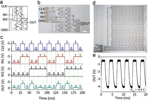
Figure 4. All-CNT logic gates and ring oscillators. a) Circuit diagram of a two-input XOR logic gate. b) Optical microscopy image of an XOR logic gate fabricated on a flexible PEN substrate (scale bar, 100 μm). c) Input–output characteristics of the XOR logic gate. d) Optical microscopy image of a 101-stage ring oscillator fabricated on a flexible PEN substrate (scale bar, 500 μm). e) Output characteristics of the ring oscillator at VDD = -4.4 V. (Image by IMR)