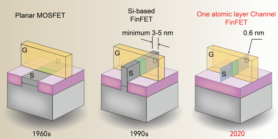
FinFETs are known to be an evolution of metal-oxide-semiconductor field effect transistors (MOSFETs) featuring a semiconducting channel vertically wrapped by conformal gate electrodes. It was first proposed in 1990s in order to avoid the short channel effect and other drawbacks resulted from the shrinking of transistor size. Because of the limitation of nanofabrication, the minimum fin width is about 5 nm in nowadays technology.
In the past decades, microelectronics has developed in a rapid pace following the Moore’s Law, with the number of transistors per area increased bi-yearly. Due to the limitation of nano-fabrication precision, it is now extremely challenging to shrink further the size of transistors on an integrated circuit. It is therefore of great importance to seek new candidates of semiconducting materials. In recent years, novel materials such as carbon nanotubes and two dimensional materials have been widely studied for the implementation of nano-scaled transistors.
Recently, led by the Institute of Metal Research, Chinese Academy of Sciences, an international research team from China and France published a research paper entitled “A FinFET with one atomic layer channel”. This work aims at replacing the conventional Si-based fin with two-dimensional single atomic layer in the FinFET architecture.
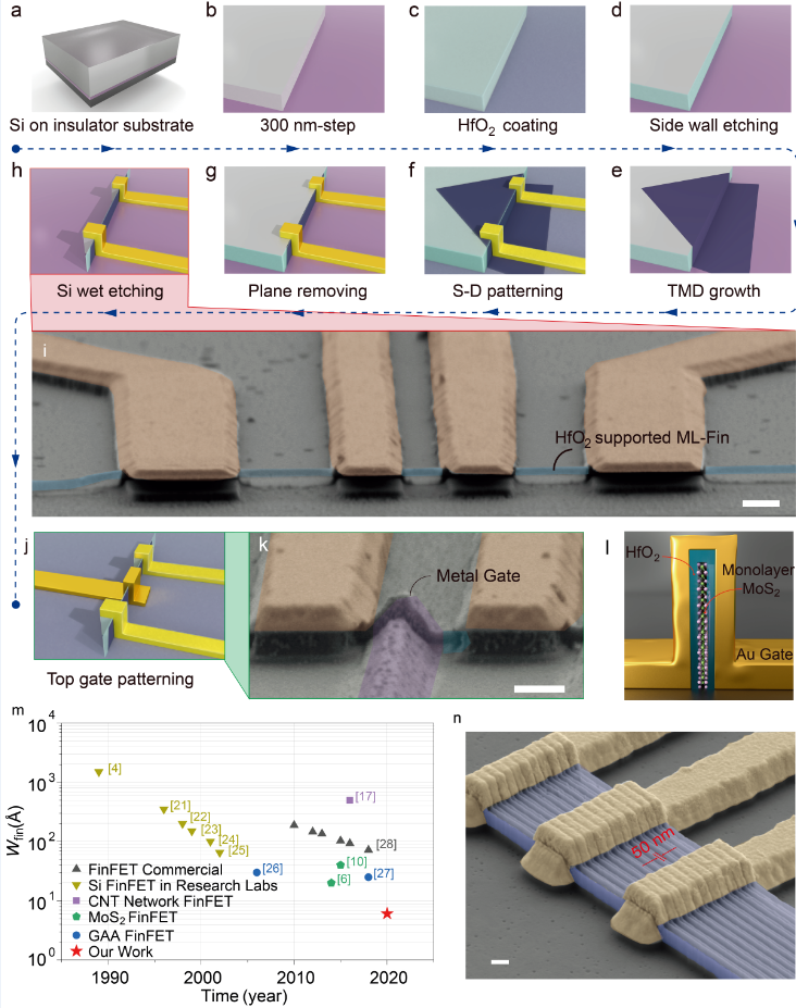
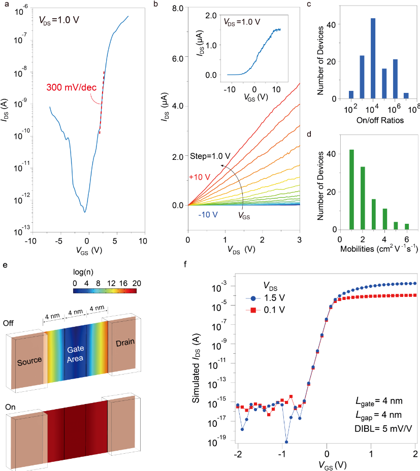
A wet-sprayed chemical vapor deposition (CVD) method was designed to universally grow monolayers of transition metal dichalcogenides (ML-TMDCs, such as MoS2, WS2, etc.) on step-shaped templates with height at the order of 300 nm. After a dedicated work flow of multiple-step etching and nano fabrication processes, vertically standing single layer MoS2 channels are successfully wrapped with dielectric and gate electrodes, with source and drain electrodes contacting the 0.6 nm fin channel. The resulted ML-FinFET structure is illustrated in Fig. 1. Gate electrodes can also be made of a carbon nanotube thin film. The best electrical performances of such ML-FinFETs are obtained to show on/off ratio reaching 10^7, sub-threshold swing of about 300 mV/dec, and mobilities at the order of a few cm^2V^-1s^-1. Simulations show that, by further optimizing the structure of the ML-FinFETs, DIBL can be lowered to 5 mV/V (Fig. 2).
As a summary, a FinFET with sub 1 nm fin width was achieved via a bottom-up route to grow monolayered (ML) MoS2 (thickness ~ 0.6 nm) as the fin, which is nearly the physical limit that one can actually achieve (Fig. 3). Fin-arrays with minimum pitch of 50 nm are also demonstrated, providing new insights for the implementation of nanoelectronics in the foreseeable future where the Moore's Law might be no longer valid.
The study has been published in the journal Nature Communications.Figure 1. a)-j) Work flow of the fabrication processes of ML-FinFET;i) and k) SEM images of the device before and after gate electrode patterning. Scale bars are500 nm;l) A schematic picture of the cross section of ML-FinFET;m) A time scale evolution of the fin-width of FinFETs;n) SEM images of the ML-Fin-arrays fabricated using the method proposed in this article. Scale bar is 50 nm. (Image by IMR)
Figure 2. a)-d) Electrical performances of the MoS2 ML-FinFETs;e)-f) Finite-element simulations of the FinFETs.(Image by IMR)
Figure 3. Different configurations of MOSFET.(Image by IMR)