Ferroelectric tunnel junction (FTJ) has a compact metal-ultrathin ferroelectric-metal stacking structure. It utilizes the switching of ferroelectric polarization to control the quantum tunneling behavior of electrons, achieving various resistance states used for data storage. It is one of the next-generation information storage technologies due to its high-speed reading and writing, low power consumption, and high storage capacity. Tunneling electroresistance (TER, or on/off ratio) is a key performance parameter, which closely relates to the interfacial charge screening and the ferroelectric polarization magnitude theoretically. At present, various electrode engineering methods have been explored to modulate the charge screening for improving TER. However, the effect of polarization magnitude on TER has yet to be experimentally verified.
Recently, a research team leading by Prof. HU Weijin, from Shenyang National Laboratory for Materials Science, Institute of Metal Research, Chinese Academy of Sciences (IMR, CAS), have proposed a new strategy that utilizes buffer layer to quantitatively control the thin-film strain and delay the lattice relaxation of ferroelectric films, thus enhancing the ferroelectric polarization and TER in the corresponding FTJs.
Researchers used the Sr3Al2O6/La0.67Sr0.33MnO3/BaTiO3 multiferroic heterostructure as a model system, and employed the laser molecular beam epitaxy technology to grow the multi-layer films layer-by-layer. They found that Sr3Al2O6 buffer-layer thickness can effectively modulate the in-plane strain state of BaTiO3 single-crystalline film, thereby substantially enhancing the ferroelectric polarization magnitude, to a record-breaking value of ~80 μC/cm2 on BaTiO3/La0.67Sr0.33MnO3 interface under a compressive strain of -2.1%. Leveraging this large polarization, they achieved a giant TER of 105 in buffered FTJ, which is 100 times larger than that of FTJ without the buffering layer.
The findings were published with the title of “Epitaxial strain enhanced ferroelectric polarization towards a giant tunneling electroresistance” in the latest issue of academic journal ACS Nano.
Prof. HU Weijin said, “Our research uncovers the fundamental interplays between strain, polarization magnitude, and FTJ device performance, and it will promote the usage of FTJs for next-generation information storage applications.”
This study was done in collaboration with Prof. YANG Teng and Prof. TANG Yunlong from IMR and other collaborators.
The work was supported by the National Key R&D Program of China (Grant No. 2022YFA1203903), the National Natural Science Foundation of China (NSFC) (Grant Nos. 61974147, 52031014), and Special Fund for Central Government Guiding the Local Development of Science and Technology (Grant No. 2023JH6/100100063).
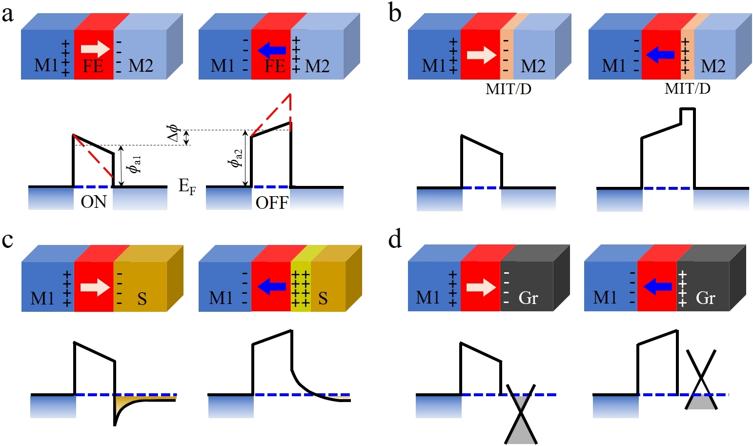
Figure 1. Different schemes for enhancing the TER effect. (a) FE polarization (P) dependent TER in metal (M1)/FE/metal (M2) FTJ. The average tunneling barriers ( and
and  ) and their difference,
  , are dependent on polarization magnitude and direction. A larger P theoretically induces a steeper barrier as indicated by red dashed lines, leading to an enhanced TER. (b) FE modulated interfacial metal-insulator transition (MIT) or FE-dielectric (D) composite tunneling barrier; (c) FE modulated barrier width through charge accumulation/depletion by using semiconducting (S) electrode; (d) FE modulated additional carrier density by using 2D Graphene (Gr) as electrode. For simplicity, M1 is assumed to be an idea metal with perfect charge screening. Arrows represent FE polarizations. (Image by IMR)
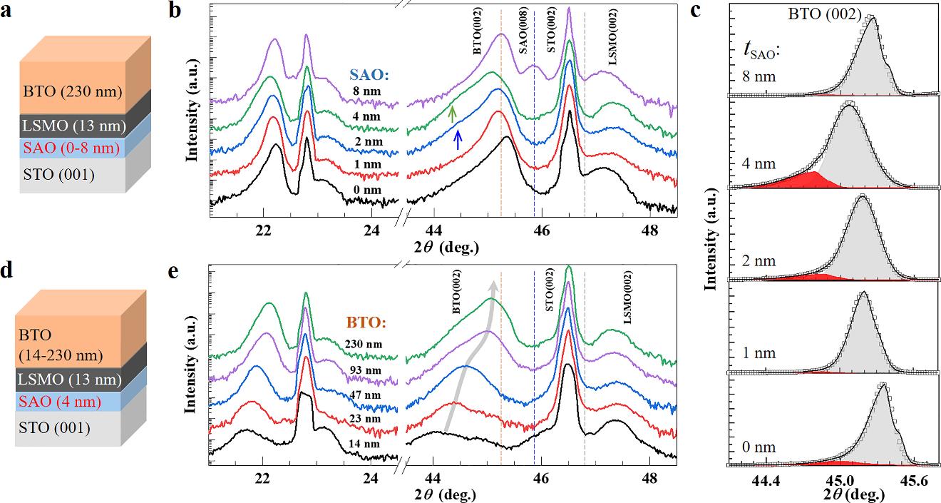
Figure 2. HRXRD of BTO films growing on LSMO/SAO/ (001) STO substrates. (a) The schematic multilayer films with varied tSAO ranging from 0 nm to 8 nm, and (b) the corresponding XRD patterns of the multilayers. Dashed lines indicate the diffraction peak positions of bulk BTO, SAO, and LSMO, respectively. (c) Enlarged (002) BTO peak with intensity in linear scale. (d) The schematic multilayer films with BTO thickness ranging from 14 nm to 230 nm while fixing tSAO at 4 nm, and (e) the corresponding XRD patterns. Grey arrow indicates the shift of BTO (002) peaks depending on thickness. (Image by IMR)
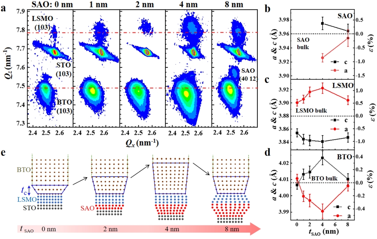
Figure 3. RSM of BTO (230 nm)/LSMO/SAO/ (001) STO with various SAO thickness. (a) RSM around (103) STO with various tSAO ranging from 0 nm to 8 nm. The horizontal dashed lines are guide to the eyes. The as-derived lattice constants (a & c, left) and strains (ε, right) as a function of tSAO for (b) SAO buffer layer, (c) LSMO bottom layer, and (d) BTO films. The dashed lines indicate lattice constants of bulks. (e) The schematic lattice strain evolution of BTO/LSMO/SAO multilayer films dependent on tSAO. An SAO layer of 4 nm gives the best lattice matching between LSMO and BTO and so delays BTO lattice relaxation. (Image by IMR)
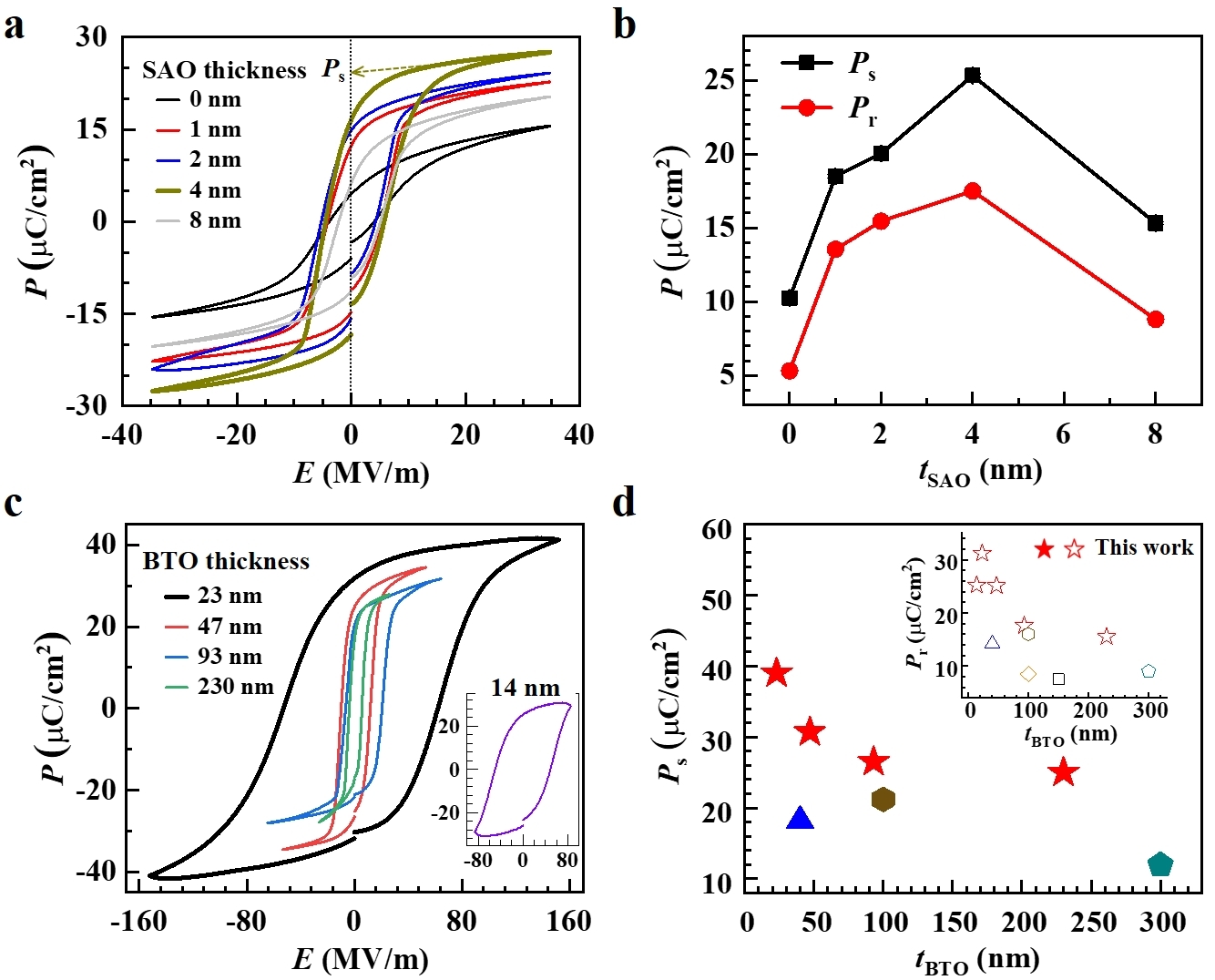
Figure 4. Ferroelectric properties of BTO films. (a) P-E loops of 230 nm BTO films with tSAO ranging from 0 to 8 nm. (b) The derived Ps and Pr as a function of tSAO. (c) P-E loops of BTO thin film capacitors with tSAO fixing at 4 nm and with BTO thickness ranging from 230 to 14 nm. (d) Ps and Pr (inset) of various BTO films growing on LSMO electrode (20, 28-31). (Image by IMR)
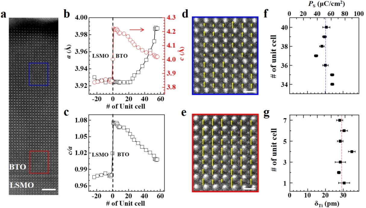
Figure 5. STEM of BTO with a thickness of 23 nm growing on LSMO/SAO/STO. (a) cross-section HRSTEM image along [100] direction. Dashed line indicates the LSMO/BTO interface. (b) lattice constants a (left) and c (right). (c) The tetragonality c/a ratio along the thickness direction across the LSMO/BTO interface as derived from (a). Twenty atomic positions have been averaged during the data acquisition. (d) and (e) are the enlarged atomic positions together with the atomic displacement mapping of Ti ions (yellow arrows) of two typical regions near and away from the LSMO/BTO interface as marked by red and blue boxes in (a). (f) and (g) show the Ti displacement δTi and the corresponding Ps along the thickness direction for the two regions. The sacle bar in (a) is 2 nm, and the scale bar in (d) & (e) is 0.5 nm. (Image by IMR)
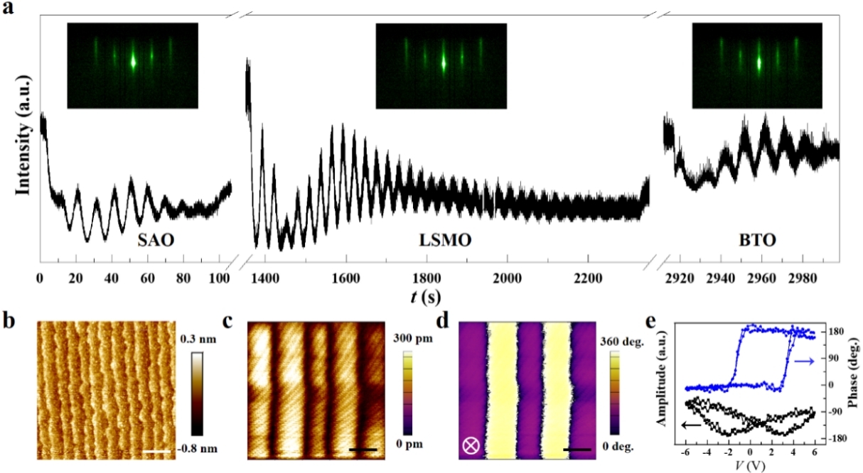
Figure 6. Ultrathin film growth and scanning probe microscopy characterization. (a) RHEED intensity oscillations of the specular reflected beam during the growth of SAO-4 nm/LSMO-13 nm/BTO-3.2 nm multilayers. Inset shows the RHEED patterns after each layer growth. (b) Topographic image, (c) OP PFM amplitude, and (d) OP PFM phase image acquired on the BTO ultrathin film. Scale bar in (b) is 500 nm, and in (c) and (d) are 1 μm. (e) Typical local PFM amplitude (black, right) and phase (green, left) hysteresis loops. Note the diagonal lines in (c) originate from the noise of the equipment during the measurement. (Image by IMR)
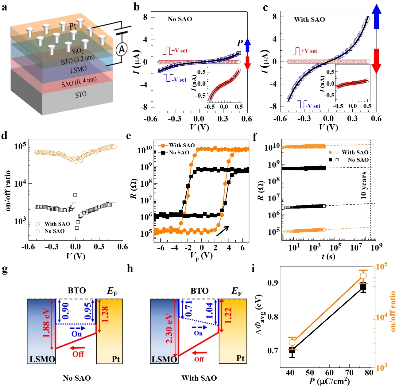
Figure 7. Buffer layer enhanced giant tunneling electroresistance. (a) the schematic FTJ device structure. I-V curves of opposite polarization states for (b) FTJ without SAO buffering layer, and (c) FTJ with SAO buffering layer. Blue and red arrows indicate the polarization direction. Black solid lines are the fittings according to the direct tunneling model. (d) On/off ratio derived from (b) and (c) for the two kinds of FTJs. (e) The resistance memory loops reading at a voltage bias of -0.2 V for typical FTJs. Black arrows indicate the writing voltage sweep direction. (f) Retention properties of the HRS and LRS after setting by +6 V and -6 V with pulse width of 1 s for typical FTJs. (g) and (h) show the corresponding band alignment for two FTJ devices, where the barrier heights are derived from the fittings in (b) and (c), respectively. (i) The tunneling barrier height difference DΦavg (left) and on/off ratio (right) as a function of polarization magnitude. The error bars represent the s.d. measured in 8 junctions for each kind of FTJ. (Image by IMR)
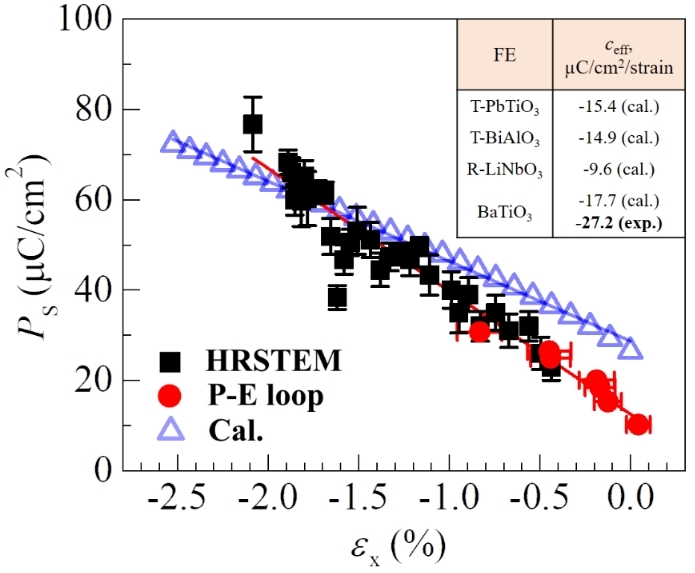
Figure 8. Spontaneous polarization Ps of BTO films as a function of in-plane epitaxial strain εx.εx are obtained both from RSM characterization (Red circle) and from HRSTEM analysis (Black square). Ps have been obtained from P-E loops (Red circle) and from HRSTEM (Black square). Red line is the linear fitting of the experimental data. Blue triangle represents the first principles calculation values for BTO. Inset table lists the strain sensitive coefficient ceff for typical ferroelectrics. (Image by IMR)