A research team has developed a novel electron tomography method that can quantitatively reveal the three-dimensional (3D) morphology and crystallographic features of grain boundaries in nanostructured metals, providing a powerful tool to understand the stability and performance of these advanced materials.
Grain boundaries are crucial defects that determine a material's strength, thermal stability, and how atoms diffuse through it. As grain size decreases to the nanometer scale, these boundaries become so numerous that their structure and behavior largely dictate the material's properties. However, directly analyzing their true 3D geometry and crystal orientation has been a long-standing challenge, as traditional microscopes only provide flat, two-dimensional projections.
To overcome this, Prof. LI Xiuyan and Prof. DU Kui from the Institute of Metal Research, Chinese Academy of Sciences (IMR, CAS), developed a technique called Dark-Field Electron Tomography for Nanograins (DFET-Nano). Using a transmission electron microscope, the team captures a series of dark-field images as the sample is tilted. By analyzing how the image intensity changes, their method simultaneously reconstructs the 3D shape of each nanograin and its crystal orientation. This allows them to calculate the crystallographic plane and curvature of the grain boundaries with an impressive spatial resolution of about 0.3 nanometers.
The team validated DFET-Nano on a nanocrystalline nickel sample with a specific "five-fold twin" structure, successfully reconstructing the grain shape and identifying its boundary as the characteristic {111} plane. They then applied it to study nanocrystalline platinum, revealing how grain boundary structures evolve during heating. As the annealing temperature increased, they observed a growing proportion of low-energy boundaries, a decrease in average boundary curvature, and a trend toward more correlated orientations between next-nearest neighbor grains. These observations visually confirm theoretical predictions about the stability of nanocrystalline structures.
This research, published in the journal Matter, provides the first direct experimental evidence of how grain boundary networks evolve in nanometals with extremely fine grains. The DFET-Nano method opens a new avenue for 3D structural characterization of nanomaterials, offering critical insights for designing more stable and higher-performance nanocrystalline materials for future applications.
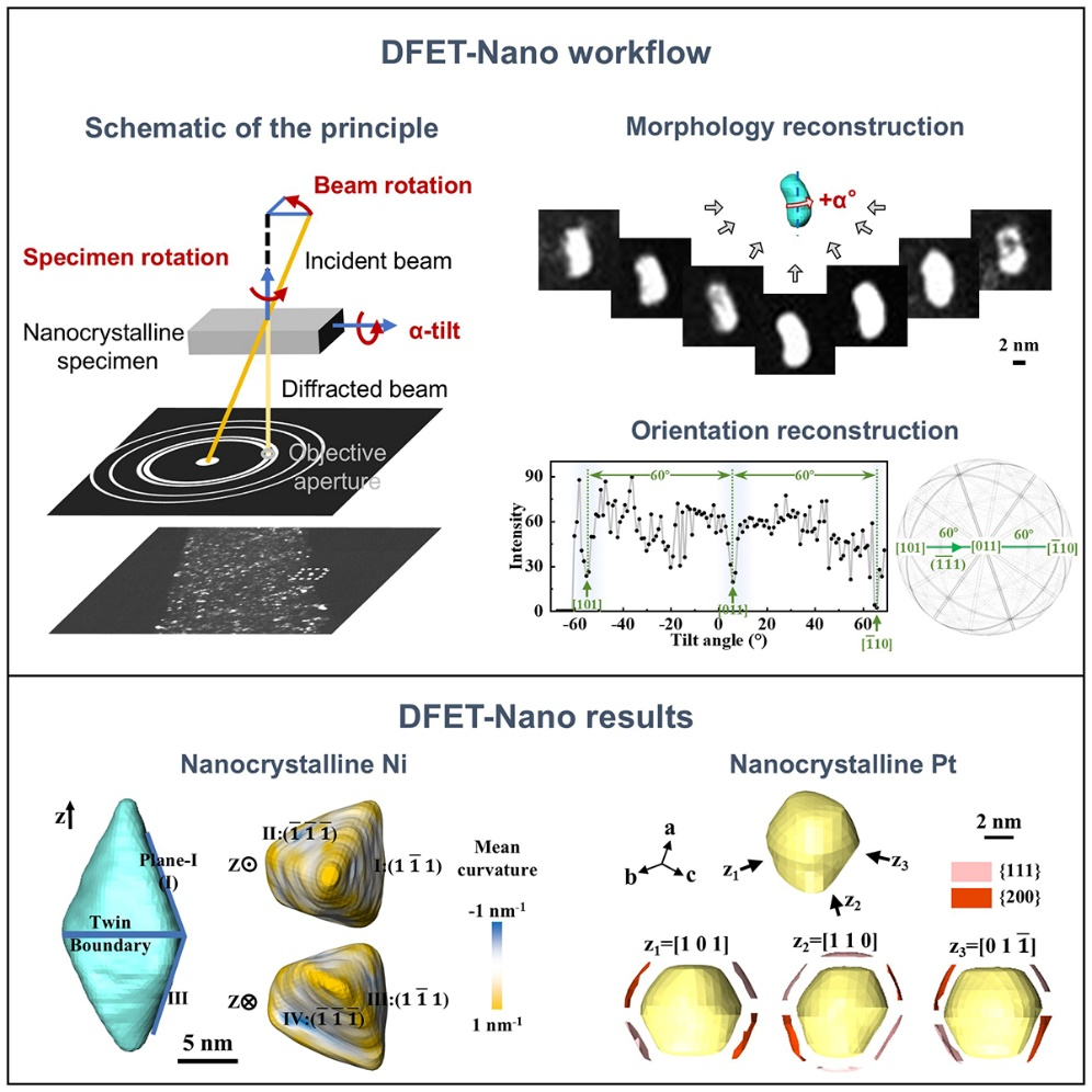
Experimental workflow of DFET-Nano and 3D reconstruction results of nanocrystalline Ni and Pt. (Image by IMR)