Scientists from the Institute of Metal Research, Chinese Academy of Sciences (IMR, CAS), in collaboration with Northeastern University and other institutions, have proposed the concept of “Optical Fiber Electronics” and demonstrated the integration of electronic, optoelectronic, and wireless functionalities on a single optical fiber. The work, published in National Science Review, extends the functionality of optical fibers beyond passive light transmission toward active information processing and external interfacing.
Optical fibers underpin the global information infrastructure owing to their exceptionally low transmission loss and enormous data-carrying capacity. However, conventional optical fibers have served primarily as passive transmission media. Signal modulation, detection, and logic operations are still performed by separate chips and systems outside the fiber. Integrating active electronic and optoelectronic functions directly onto the fiber surface could transform the fiber into a multifunctional information platform.
The team used a D-shaped optical fiber as the integration platform and developed micro/nanofabrication processes tailored to its side-polished surface. They first integrated high-density carbon nanotube thin-film transistors and logic circuits on the fiber surface, realizing on-fiber electronic logic functions. In addition, quantum-dot/carbon-nanotube phototransistors were fabricated to enable in situ detection of guided optical signals through evanescent-field coupling. The devices achieved maximum specific detectivities of 3.82 × 10¹⁶ Jones under external illumination and 3.25 × 10¹⁵ Jones under waveguide-coupled illumination. By combining photodetection with electronic logic, the team further demonstrated optically controlled logic inversion on the fiber while maintaining continuous propagation of the guided optical signal. They also fabricated multilayer microcoils on the fiber surface to enable wireless communication capability. Through near-field magnetic coupling, the system achieved sub-meter-scale wireless power transfer, producing a measurable DC voltage after rectification at a distance of 60 cm. The microcoils also enabled radio-frequency signal emission with a stable response over the 500 kHz–13.56 MHz range.

Optical fiber electronics for multifunctional device integration. (a) Schematic of a conventional fiber-optic communication system; (b) Schematic of the optical fiber electronics concept; (c) Optical micrograph of multiple functional devices integrated on the surface of a D-shaped optical fiber. (Image by IMR)
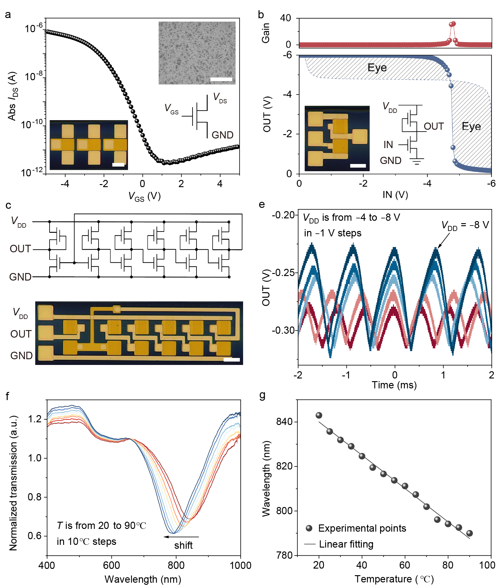
On-fiber transistors and logic circuits. (a) Transfer characteristics of carbon nanotube thin-film transistors; (b) Input–output characteristics and voltage gain of the inverter; (c) Circuit diagram of a five-stage ring oscillator; (d) Optical micrograph of the five-stage ring oscillator; (e) Output waveforms of the ring oscillator under different supply voltages; (f) Transmission spectra of the optical fiber at different temperatures; (g) Temperature response of the surface plasmon resonance wavelength. (Image by IMR)

On-fiber phototransistors and detection performance. (a) Structure of the CsPbBr₃ quantum dot/carbon nanotube phototransistor; (b) Cross-sectional transmission electron micrograph of the device; (c) Transfer characteristics under external illumination; (d) Transfer characteristics of the device under waveguide-coupled illumination; (e–g) Key photodetection performance metrics as functions of optical power density: (e) responsivity; (f) external quantum efficiency; (g) specific detectivity; (h) Benchmarking against representative photodetectors. (Image by IMR)
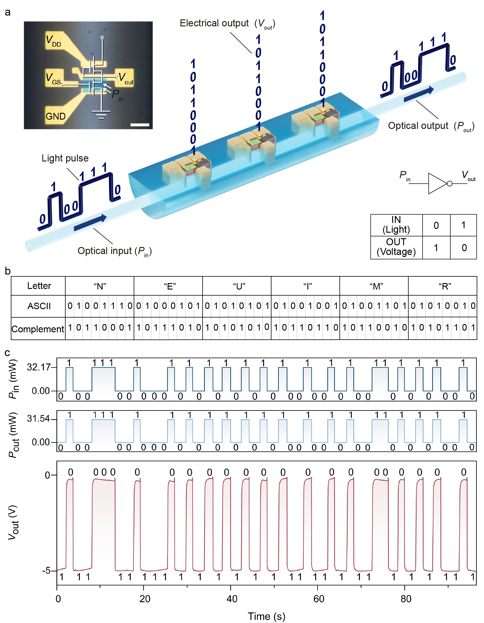
On-fiber optically controlled logic functions. (a) Optically controlled logic inverter driven by the evanescent field of the guided mode; (b) ASCII bit encoding of the characters “NEU-IMR”; (c) Optical input, optical output and inverted electrical logic output. (Image by IMR)
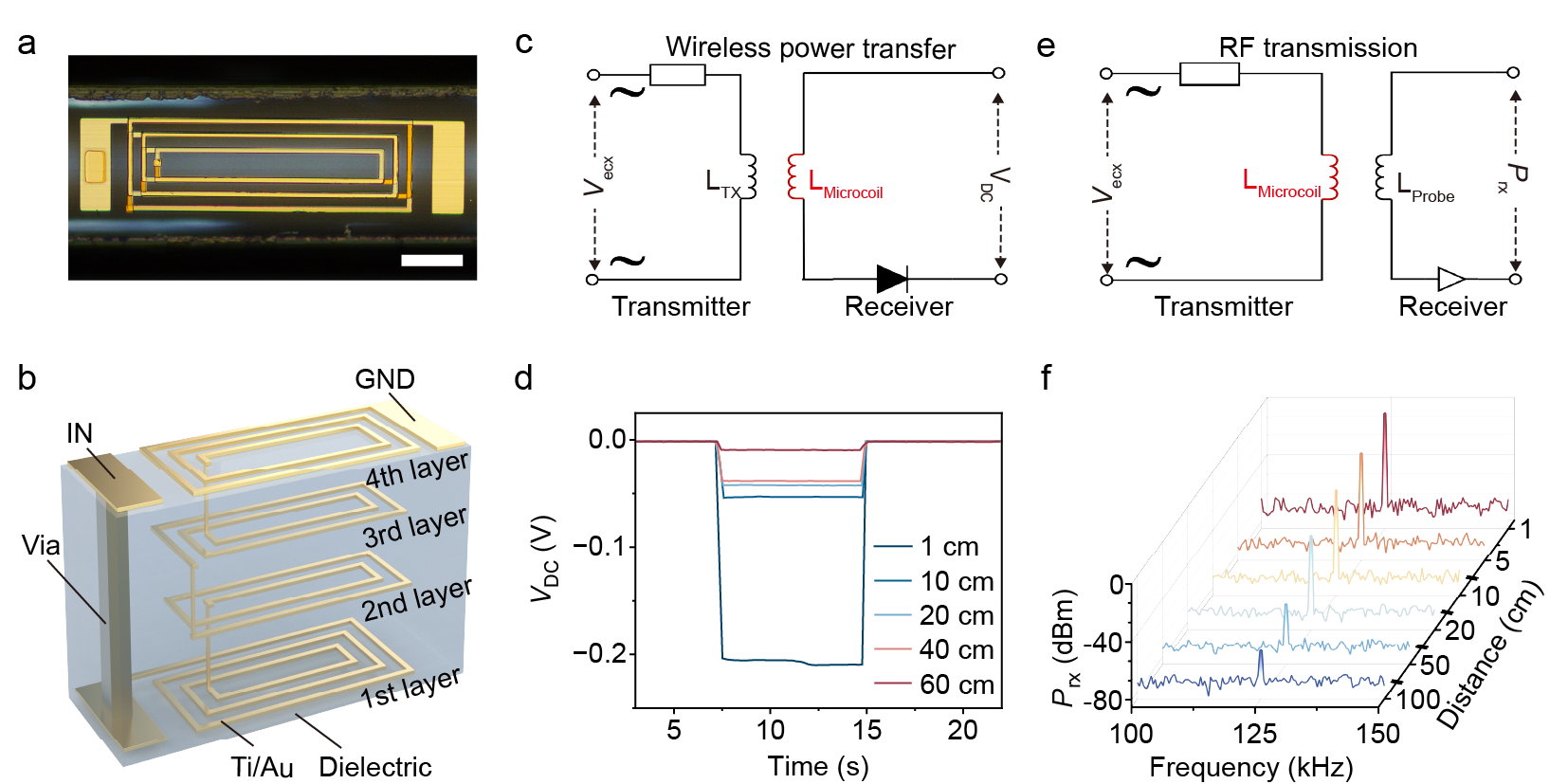
On-fiber wireless communication functions. (a) Optical micrograph of the microcoil; (b) Multilayer microcoil structure; (c) Equivalent circuit for wireless power transfer; (d) Induced voltage at different transmission distances; (e) Equivalent circuit for radio-frequency signal emission; (f) Received spectra at different transmission distances. (Image by IMR)